
News Center
新闻中心
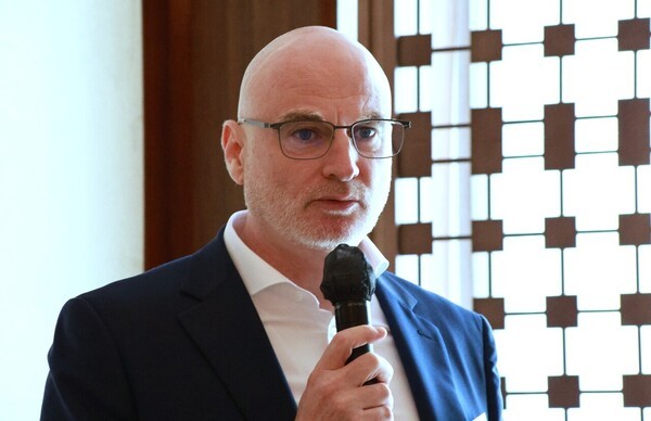
German optics giant ZEISS has officially opened the "ZEISS Semiconductor Innovation Center" in Yongin, Gyeonggi Province, South Korea, marking the company's first semiconductor R&D facility in the country.
The center will be staffed with top engineering talent focused on developing next-generation extreme ultraviolet (EUV) lithography optical systems and optimizing wafer inspection solutions. It will provide advanced optical solutions support for Korean chipmakers including Samsung Electronics and SK hynix.
A ZEISS Semiconductor Manufacturing Technology representative stated: "Korea is a vital base for global semiconductor manufacturing. Establishing this innovation center will allow us to work more closely with customers and accelerate the development and application of next-generation lithography technology."
Industry analysts noted that as chip manufacturing processes continue advancing toward more sophisticated nodes, the importance of EUV lithography technology grows increasingly prominent.


 WeChat